Email US:info@kartain.com
|
|||||||||||||||||||||||||||
Product Description Contact Us
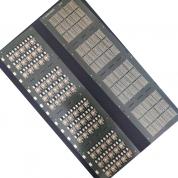
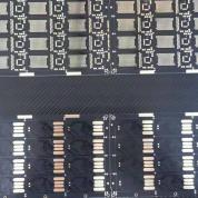
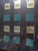
What is FCPGA/FCCSP PCB---IC substrate PCB CHINA
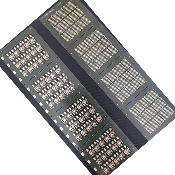
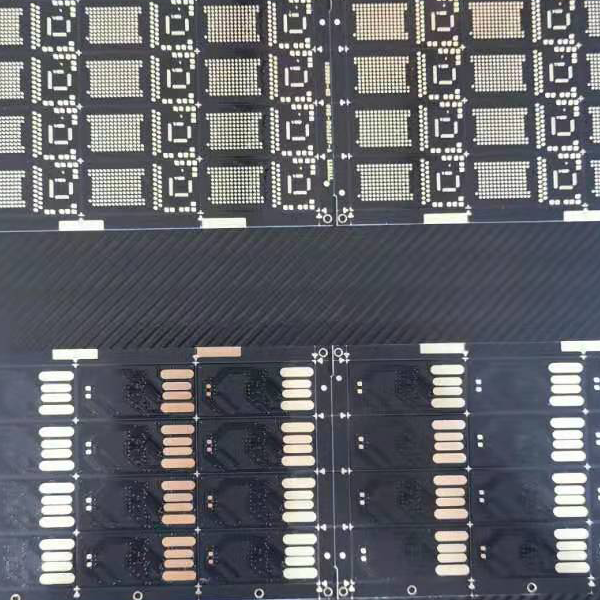
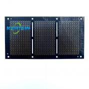
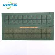
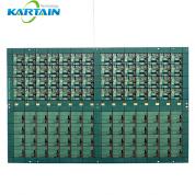
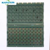
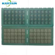
Flip Chip BGA (FCBGA) packages are assembled around state‑of‑the‑art, single unit laminate or ceramic substrates. Utilizing multiple high density routing layers, laser drilled blind, buried and stacked vias, and ultra fine line/space metallization, FCBGA substrates have the highest routing density available. By combining flip chip interconnect with ultra advanced substrate technology, FCBGA packages can be electrically tuned for maximum electrical performance. Once the electrical function is defined, the design flexibility enabled by flip chip also allows for significant options in final package design. Kartain offers FCBGA packaging in a variety of product formats to fit a wide range of end application requirements.
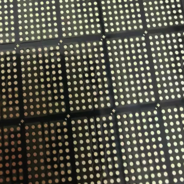
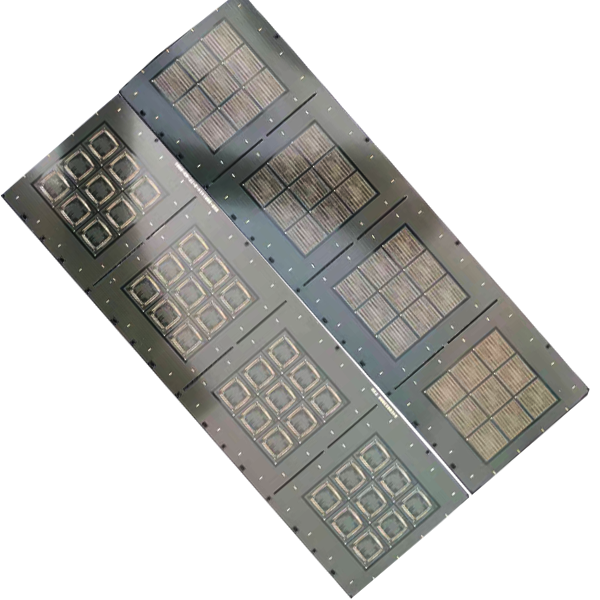
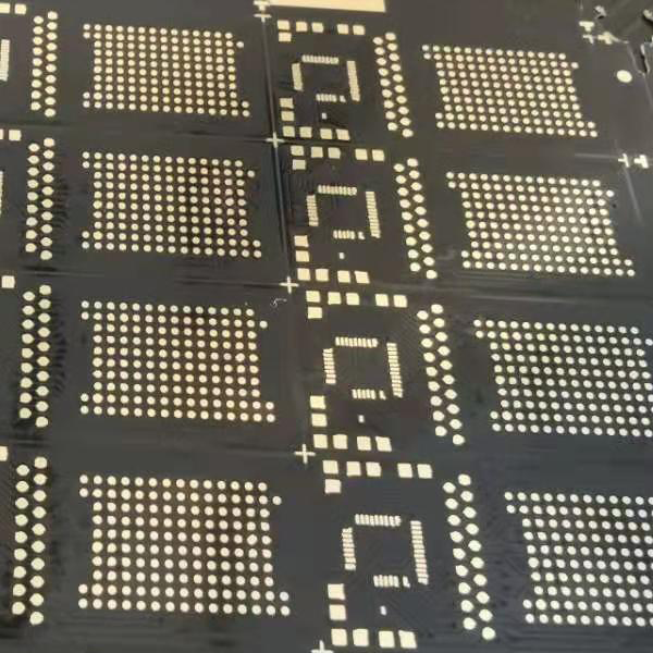
FCBGA/FCCSP ABF package pcb boards Technology Solutions
Substrates
4-18 layer laminate build-up substrates
High CTE ceramic
Coreless
Bump Types
Eutectic Sn/Pb
Pb-free (green)
Cu pillar (array and fine pitch peripheral)
Package Formats
Bare die
Lidded
FCBGA/FCCSP ABF package pcb boards production capacity
| Process capability | |
| Item | Capability |
| Material | Shengyi,BT,Mitsubishi,Toshiba,LG |
| Layers | 1-8layer |
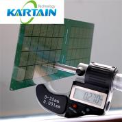
| Min Boards thk | 2layer--0.1mm |
| 4layer--0.18mm | |
| 6layer--0.26mm | |
| Min Vias/blind vias | 100um/55um |
| Min Line spacing/Width | 25um/25um |
| Copper Weight | 8-35um,70um |
| Surface finished | ENIG,NiPdAu,Immersion Silver |
| Soldermask | Black Taiyo soldermask,White,Red,Yellow,Blue soldermask |
| Special technics | Tenting/Etech back/Buss-less/MSAP/Plugged |
| Application | Semiconductor Integrated Circuit,MEMS,Antenna,Medical equipment,RAM,SD ,SSD,Camera,Fingerprint Recognition,IC substrate package |
| Min drilling vias | 0.05mm |
| Min pad gap | 0.05mm |
| IC substrate package | UDP,CSP,SIP,FMC,LGI,PBGA,SSD,MEMS,MiniLED,SSOP,TSOP,QFP,TQFP |
The special testing for FCBGA/FCCSP ABF package pcb boards
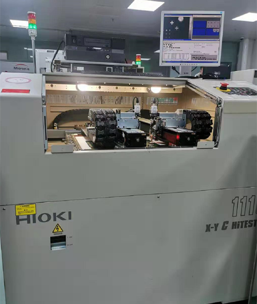
1116 X-Y C HiTESTERis a non-fixture testing
And we can supply the FCBGA/FCCSP ABF package pcb boards with ABF material,
the 4layer pcb thickness reach to 0.2mm.
CONTACT KARTAIN TECHNOLOGY
Kartain is committed to to provide you with exceptional support and satisfaction for your PCB fabrication and PCB assembly needs from QTA prototyping to High volume production.
Our experts are available to consult you for your project. So, call us anytime at 0755-23024958 or get in touch via email.
More Contact Info:
KARTAIN Factory: #3RD BUILDING HONGCHONG INDUSTRIAL DISTRICT HONGXING SONGGANG TOWN BAOAN,SHENZHEN,GUANGDONG,CHINA-518104
Office:#212 Shuiyuanju Building,Bao'an East ,Shajing Town,Bao'an District,Shenzhen,China.
Tel: +0086(755)2302 4958, 015814406156 wechat: 409387861
Fax:+0086(755)2302 4958
Email: info@kartain.com
Skype: chinacircuit
Whatsapp: +86015814406156
Website: www.kartain.com www.kartainpcb.com www.kartainfpc.com
Facebook:https://www.facebook.com/chinapcbmanufacturer/
LinkedIn: https://www.linkedin.com/in/kartainpcb/

CopyRight 2015-2020 Kartain Technology CO.,LTD
Office Addrsss:#3RD BUILDING HONGCHONG INDUSTRIAL DISTRICT HONGXING SONGGANG TOWN BAOAN,SHENZHEN,GUANGDONG,CHINA-518104
Zip code:518104
Tel:15814406156
Website: www.kartain.com,www.kartain-tech.com
More contact infomation pls view "Contact US"




 German
 Spanish
 French
 Italian
 Portuguese
 Japanese
 Korean
 Arabic
 Russian
 Indonesian
 Vietnamese
 Send Email
 PCB业务
PCB业务 kartain pcb msn
 kartain pcb on skype


