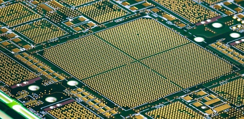
What is the HDI(High Density Interconnect) PCB boards
What is the HDI(High Density Interconnect) PCB boards
High density interconnects (HDI) PCB, represent one of the fastest-growing technologies in PCBs. Because of its higher circuitry density than traditional circuit boards, the HDI PCB design can incorporate smaller vias and capture pads, and higher connection pad densities. HDI Boards contain blind and buried vias and often contain micro vias of 0.006 or less in diameter.
By using HDI technology, designers now can place more components on both sides of the raw PCB if desired. Now as the development of via in pad and blind via technology, it allows designers to place smaller components closer together. This means faster transmission of signals and a significant reduction in signal loss and crossing delays.

HDI PCB is frequently found in mobile phones, touch-screen devices, laptop computers, digital cameras, 4G network communications, also prominently featured in medical devices.
Advantages of HDI PCB
The most common reason for using HDI technology is a significant increase in packaging density. The space obtained by finer track structures is available for components. Besides, overall space requirements are reduced will result in smaller board sizes and fewer layers.
Usually FPGA or BGA are available with 1mm or less spacing. HDI technology makes routing and connection easy, especially when routing between pins.
Function improved by HDI PCB:
1.Denser trace routing
2.More stable power
3.Reduce interference inductance and capacitance effects
4.Improve signal integrity in high-speed design
Accelerate Development with HDI Printed Circuit Boards
1.Easier to place SMD components
2.Faster routing
3.Reduce frequent relocation of components
4.More component space (also by Via-in-Pad)
Our HDI PCB manufacturing capabilities in the following table:
| Feature | Capability |
| Number of Layers | 4-30 layer |
| Quality Grade | IPC 6012 Class 2,IPC 6012 Class 3 |
| Material | Tg 140°C FR4,Tg 150°C FR4,Tg 170°C FR4 ,Special material |
| Thickness | 0.1-6.0mm, we can make the 4layer PCB as 0.1mm |
| Min Track/Spacing | Inner layer: Part 2 / 2mil, overall 3 / 3mil (H/H OZ base copper) Outer layer: Part 2.5/2.5mil, overall 3 / 3mil(H/H OZ base copper) |
| Min Hole Size | 0.15mm-0.3mm |
| Solder Mask | Green, Red, Yellow, Blue, White, Black, Purple, Matte Black, Matte green |
| Silkscreen | White, Black,Yellow,Blue |
| Surface Finish | Immersion gold,OSP,Hard gold,Immersion Silver |
| Finished Copper | 0.5-13oz |
| Build time | 5-10 days |
Lead tim |
2-3 days |
CopyRight 2015-2020 Kartain Technology CO.,LTD
Office Addrsss:#3RD BUILDING HONGCHONG INDUSTRIAL DISTRICT HONGXING SONGGANG TOWN BAOAN,SHENZHEN,GUANGDONG,CHINA-518104
Zip code:518104
Tel:15814406156
Website: www.kartain.com,www.kartain-tech.com
More contact infomation pls view "Contact US"


 German
 Spanish
 French
 Italian
 Portuguese
 Japanese
 Korean
 Arabic
 Russian
 Indonesian
 Vietnamese
 Send Email
 PCB业务
PCB业务 kartain pcb msn
 kartain pcb on skype


